- 您现在的位置:买卖IC网 > Sheet目录313 > AT27LV020A-12JU (Atmel)IC OTP 2MBIT 120NS 32PLCC
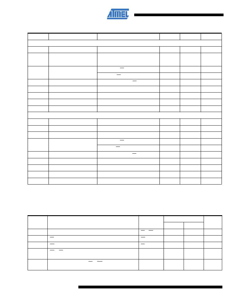
Table 5-3.
DC and operating characteristics for read operation
Symbol
Parameter
Condition
Min
Max
Units
V CC = 3.0V to 3.6V
I LI
I LO
Input load current
Output leakage current
V IN = 0V to V CC
V OUT = 0V to V CC
± 1
± 5
μA
μA
I PP1
(2)
V PP read/standby current
(1)
V PP = V CC
10
μA
I SB
I CC
V IL
V IH
V OL
V CC standby current (1)
V CC active current
Input low voltage
Input high voltage
Output low voltage
I SB1 (CMOS), CE = V CC ? ± 0.3V
I SB2 (TTL), CE = 2.0 to V CC + 0.5V
f = 5MHz, I OUT = 0mA, CE = V IL
I OL = 2.0mA
-0.6
2.0
20
100
8
0.8
V CC + 0.5
0.4
μA
μA
mA
V
V
V
V OH
Output high voltage
I OH = -2.0mA
2.4
V
V CC = 4.5V to 5.5V
I LI
I LO
Input load current
Output leakage current
V IN = 0V to V CC
V OUT = 0V to V CC
± 1
± 5
μA
μA
I PP1
(2)
V PP read/standby current
(1)
V PP = V CC
10
μA
I SB
I CC
V IL
V IH
V OL
V CC standby current (1)
V CC active current
Input low voltage
Input high voltage
Output low voltage
I SB1 (CMOS), CE = V CC ± 0.3V
I SB2 (TTL), CE = 2.0 to V CC + 0.5V
f = 5MHz, I OUT = 0mA, CE = V IL
I OL = 2.1mA
-0.6
2.0
100
1
25
0.8
V CC + 0.5
0.4
μA
mA
mA
V
V
V
V OH
Output high voltage
I OH = -400μA
2.4
V
Notes:
1. V CC must be applied simultaneously with or before V PP , and removed simultaneously with or after V PP .
2. V PP may be connected directly to V CC , except during programming. The supply current would then be the sun of I CC and I PP .
Table 5-4.
AC characteristics for read operation
V CC = 3.0V to 3.6V and 4.5V to 5.5V
Atmel AT27LV020A-12
Symbol
t ACC (3)
t CE (2)
t OE (2)(3)
Parameter
Address to output delay
CE to output delay
OE to output delay
Condition
CE = OE = V IL
OE = V IL
CE = V IL
Min
Max
120
120
50
Units
ns
ns
ns
t DF (4)(5)
t OH
OE or CE high to output float,
whichever occurred first
Output hold from address, CE or OE,
hichever occurred first
0
40
ns
ns
4
Atmel AT27LV020A
0549H–EPROM–4/11
发布紧急采购,3分钟左右您将得到回复。
相关PDF资料
AT27LV040A-90JU
IC OTP 4MBIT 90NS 32PLCC
AT27LV256A-90JU
IC OTP 256KBIT 90NS 32PLCC
AT27LV512A-90JU
IC OTP 512KBIT 90NS 32PLCC
AT27LV520-90XI
IC OTP 512KBIT 90NS 20TSSOP
AT28BV256-20SU
IC EEPROM 256KBIT 200NS 28SOIC
AT28BV64-30TI
IC EEPROM 64KBIT 300NS 28TSOP
AT28C010E-20TI
IC EEPROM 1MBIT 200NS 32TSOP
AT28C16E-15SC
IC EEPROM 16KBIT 150NS 24SOIC
相关代理商/技术参数
AT27LV020A-12JU-T
功能描述:120NS, PLCC, IND TEMP, GREEN 制造商:microchip technology 系列:- 包装:剪切带(CT) 零件状态:在售 存储器类型:非易失 存储器格式:EPROM 技术:EPROM - OTP 存储容量:2Mb (256K x 8) 写周期时间 - 字,页:- 访问时间:120ns 存储器接口:并联 电压 - 电源:3 V ~ 3.6 V,4.5 V ~ 5.5 V 工作温度:-40°C ~ 85°C(TC) 安装类型:表面贴装 封装/外壳:32-LCC(J 形引线) 供应商器件封装:32-PLCC 标准包装:1
AT27LV020A-12TC
功能描述:IC OTP 2MBIT 120NS 32TSOP RoHS:否 类别:集成电路 (IC) >> 存储器 系列:- 标准包装:32 系列:- 格式 - 存储器:闪存 存储器类型:FLASH 存储容量:1M (128K x 8) 速度:120ns 接口:并联 电源电压:2.7 V ~ 3.6 V 工作温度:0°C ~ 70°C 封装/外壳:32-LCC(J 形引线) 供应商设备封装:32-PLCC 包装:管件 其它名称:AT49BV00112JC
AT27LV020A-12TI
功能描述:可擦除可编程ROM 2Mb (256Kx8) OTP 3V 120ns RoHS:否 制造商:Maxim Integrated 类型: 存储容量:1024 bit 组织:1 K x 1 接口类型: 工作电流:5 uA 编程电压: 工作电源电压:2.8 V to 6 V 最大工作温度:+ 85 C 安装风格:Through Hole 封装 / 箱体:TO-92
AT27LV020A-12TU
功能描述:可擦除可编程ROM 2Mb (256Kx8) OTP 3V 120ns RoHS:否 制造商:Maxim Integrated 类型: 存储容量:1024 bit 组织:1 K x 1 接口类型: 工作电流:5 uA 编程电压: 工作电源电压:2.8 V to 6 V 最大工作温度:+ 85 C 安装风格:Through Hole 封装 / 箱体:TO-92
AT27LV020A-12VC
功能描述:IC OTP 2MBIT 120NS 32VSOP RoHS:否 类别:集成电路 (IC) >> 存储器 系列:- 标准包装:32 系列:- 格式 - 存储器:闪存 存储器类型:FLASH 存储容量:1M (128K x 8) 速度:120ns 接口:并联 电源电压:2.7 V ~ 3.6 V 工作温度:0°C ~ 70°C 封装/外壳:32-LCC(J 形引线) 供应商设备封装:32-PLCC 包装:管件 其它名称:AT49BV00112JC
AT27LV020A-12VI
功能描述:可擦除可编程ROM 2Mb (256Kx8) OTP 3V 120ns RoHS:否 制造商:Maxim Integrated 类型: 存储容量:1024 bit 组织:1 K x 1 接口类型: 工作电流:5 uA 编程电压: 工作电源电压:2.8 V to 6 V 最大工作温度:+ 85 C 安装风格:Through Hole 封装 / 箱体:TO-92
AT27LV020A-15JC
功能描述:可擦除可编程ROM 2M bit RoHS:否 制造商:Maxim Integrated 类型: 存储容量:1024 bit 组织:1 K x 1 接口类型: 工作电流:5 uA 编程电压: 工作电源电压:2.8 V to 6 V 最大工作温度:+ 85 C 安装风格:Through Hole 封装 / 箱体:TO-92
AT27LV020A-15JI
功能描述:IC OTP 2MBIT 150NS 32PLCC RoHS:否 类别:集成电路 (IC) >> 存储器 系列:- 标准包装:32 系列:- 格式 - 存储器:闪存 存储器类型:FLASH 存储容量:1M (128K x 8) 速度:120ns 接口:并联 电源电压:2.7 V ~ 3.6 V 工作温度:0°C ~ 70°C 封装/外壳:32-LCC(J 形引线) 供应商设备封装:32-PLCC 包装:管件 其它名称:AT49BV00112JC
